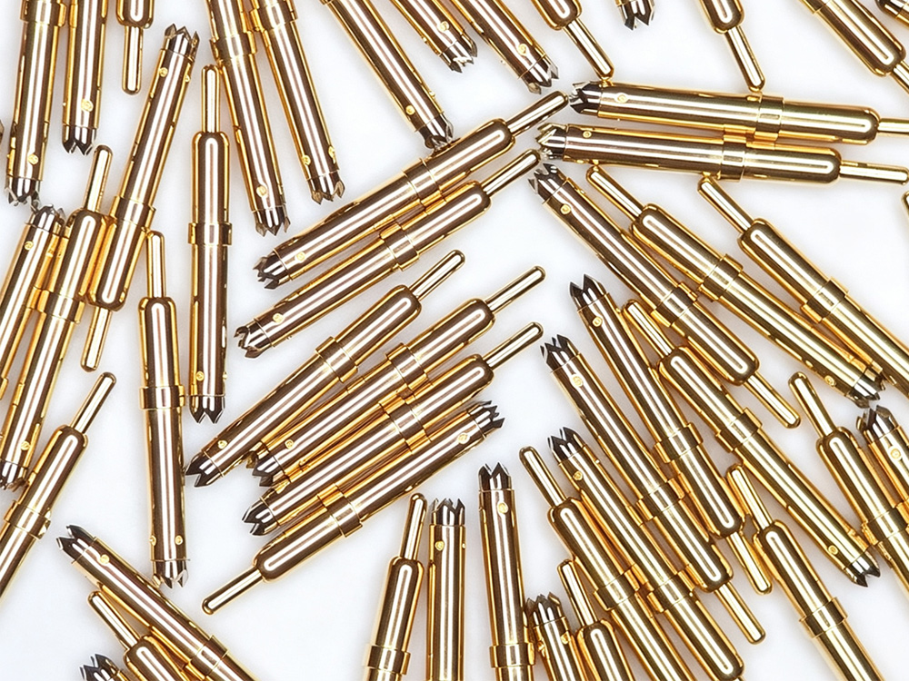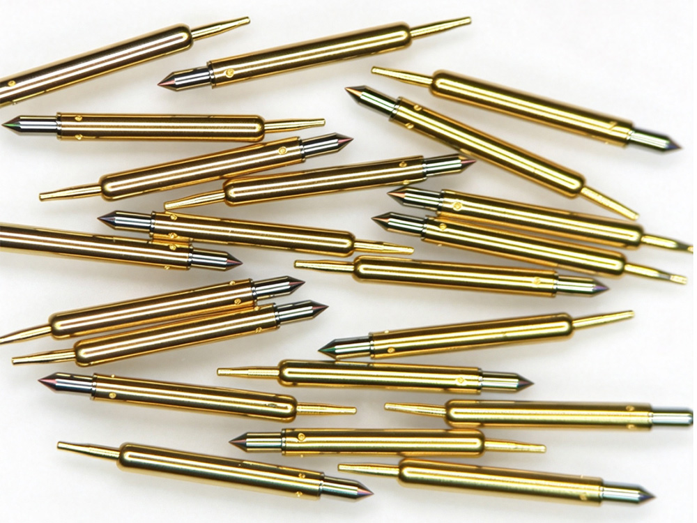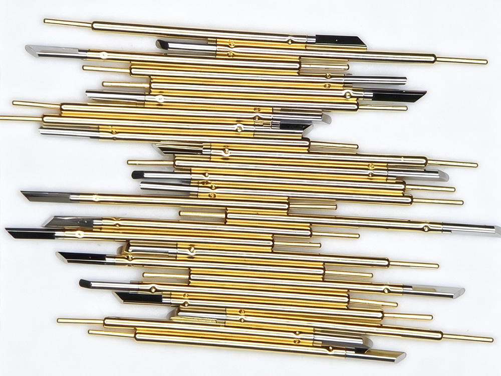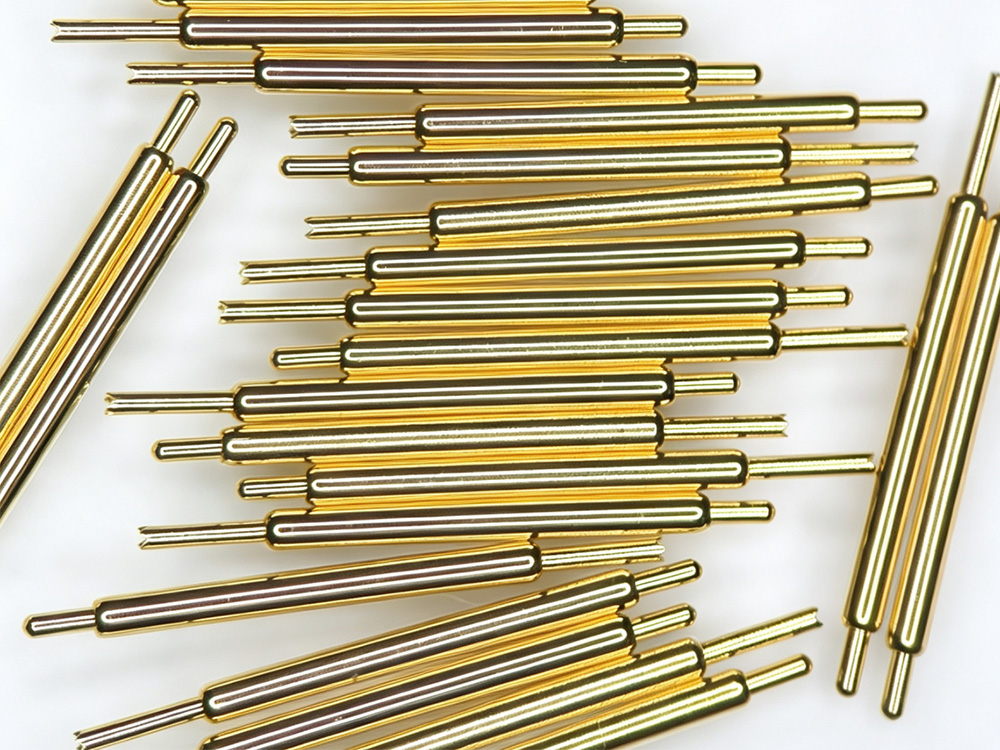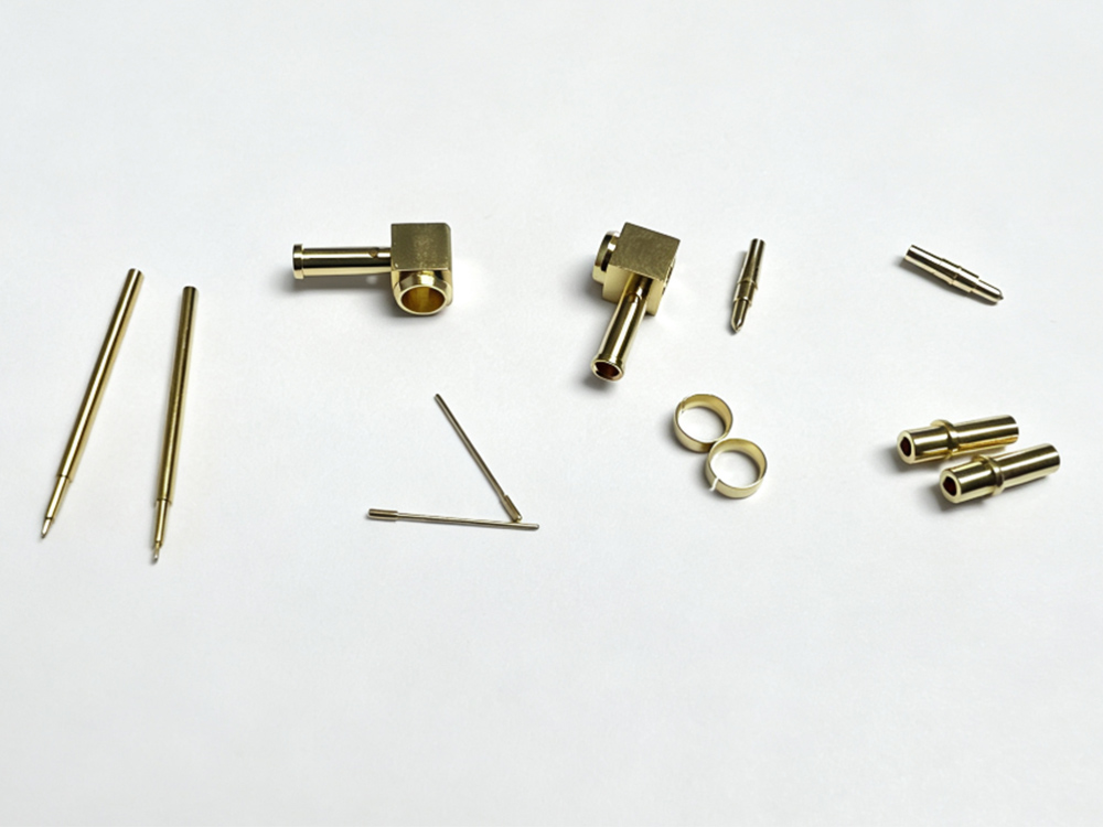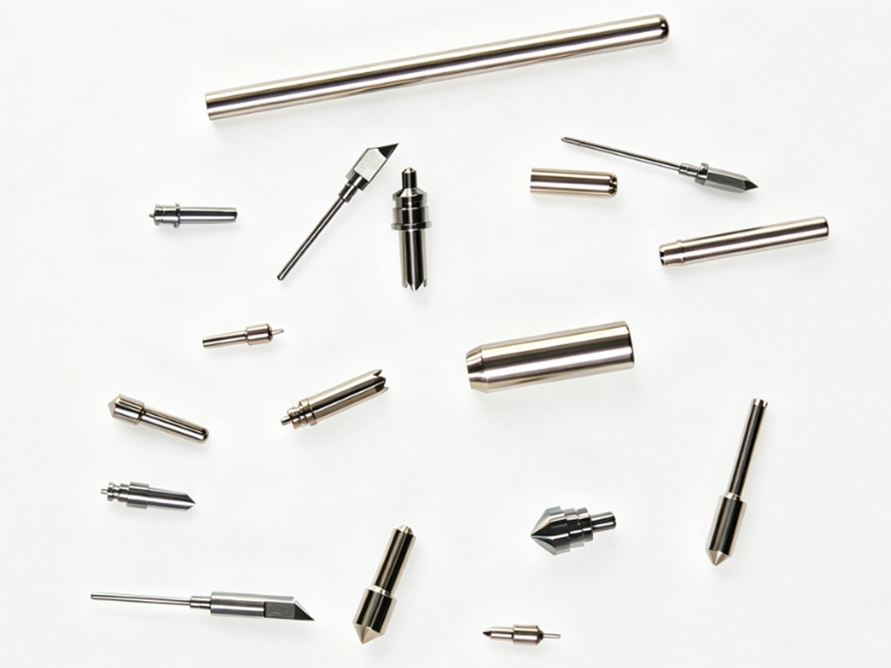
We provide customized services, different types of product chains, and offer the best solutions to satisfy every customer!
Keend focuses on project consulting, product customization, and fast delivery, providing customers with a complete set of landing service support.
Technical docking and scheme evaluation
On demand development and adaptation to various application scenarios
Efficient production scheduling and fastest delivery in 2 weeks
Pay attention to the latest developments in Keene testing technology/seize industry opportunities
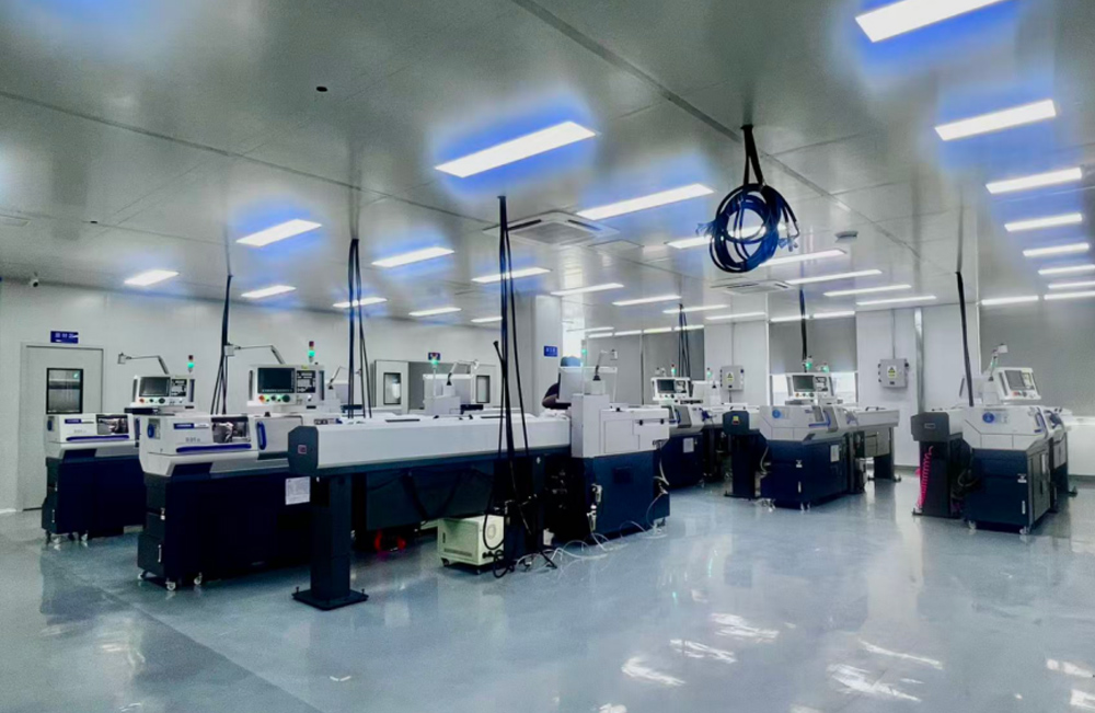

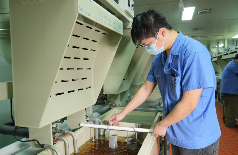


Based on precision machining, precision electroplating, microassembly, and a comprehensive precision quality control system, Jiande has built its core technological strength in chip testing probes.
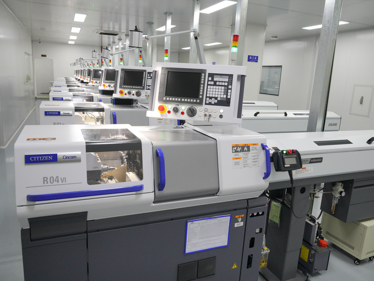
Equipped with high-end CNC machining equipment and mature advanced processing technology, relying on digital systems to achieve full process automation and precision production:
● High end CNC equipment:
equipped with cutting-edge CNC machine tools and mature standardized precision machining processes;
● Digital control:
using CAD/CAM integrated system, fully automatic control of the entire machining process;
● Ultra high machining level:
achieving industry-leading micrometer level machining accuracy, meeting the strict tolerance requirements of small parts;
● Automated production mode:
24/7 automated continuous operation, stable delivery of large quantities of high-precision products.
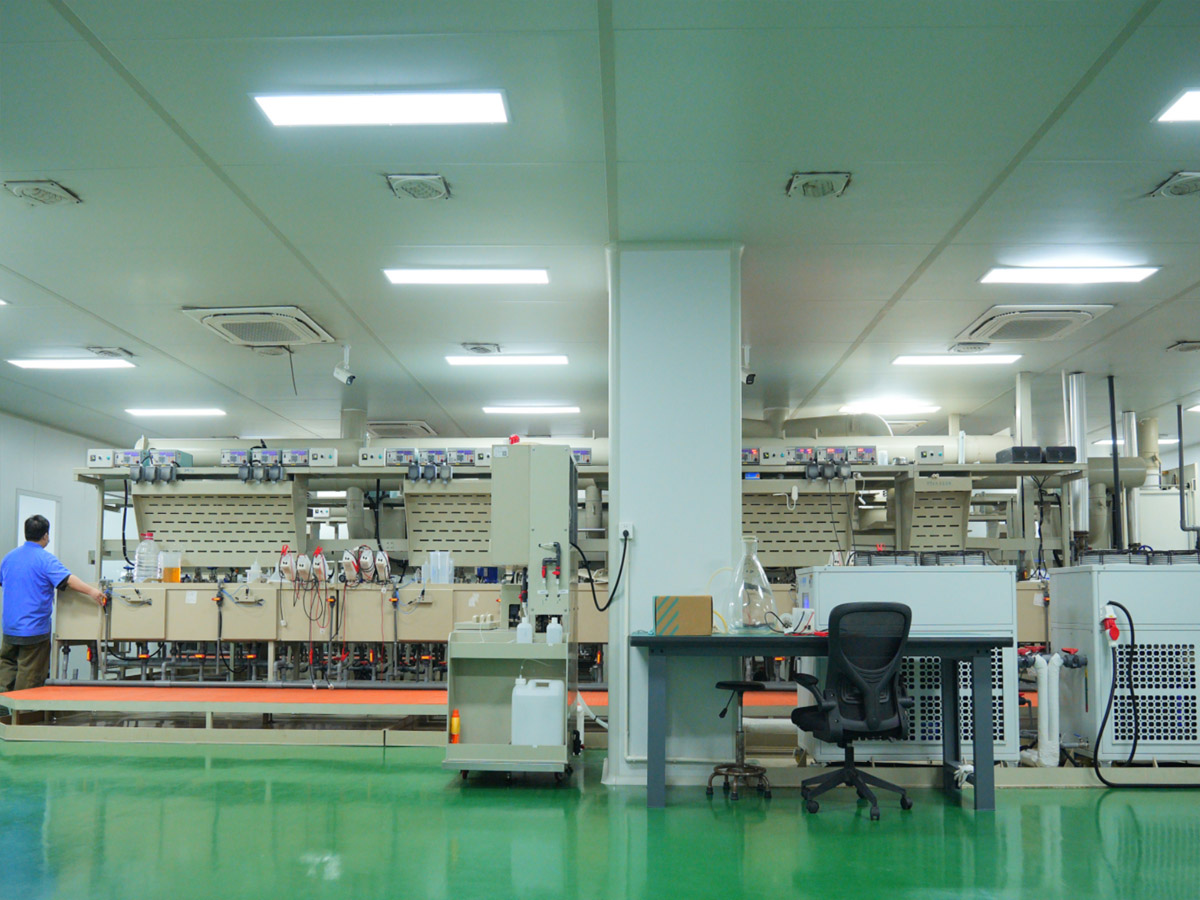
We have independently developed a complete set of precision electroplating production lines, which can achieve high difficulty electroplating processing of small parts, fine diameter needle tubes, etc., covering multiple coatings and supporting surface treatment processes:
● Hard gold electroplating:
specializing in electroplating small inner diameter needle tubes and micro precision parts, overcoming the difficult problem of coating processing for micro parts, mature landing probe dedicated hard gold plating process, with a minimum diameter of 0.10mm for gold-plated needle tubes;
● Diversified plating process:
copper plating, nickel plating, hard gold plating, palladium alloy plating;
● Supporting special technology:
exclusive special heat treatment suitable for beryllium copper, stainless steel, and palladium alloy materials; Various surface finishing treatments including fine polishing, micro polishing, and chemical polishing; High precision surface deburring precision machining;
Relying on complete electroplating and post-treatment processes, it meets the high standard coating requirements of precision components such as probes and micro pipes.
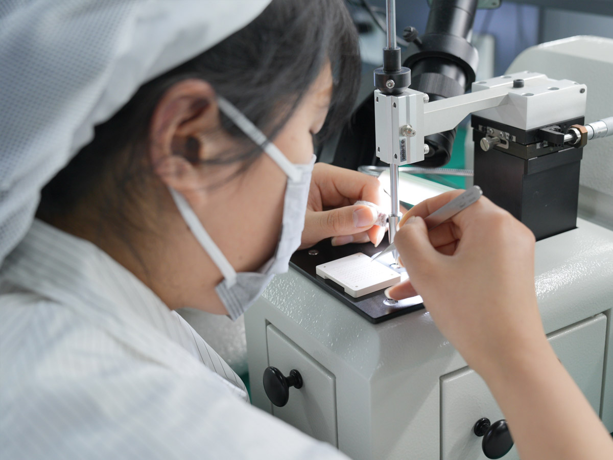
Deeply cultivating the core technology of probe microassembly, independently developing specialized assembly equipment and customized solutions, and completing the integrated precision molding of micro probe components in one stop, with multiple control systems synchronously ensuring installation:
● Fine grained micro assembly process, suitable for extremely small size assembly requirements of various micro probes such as single needle, multi needle array, integrated needle holder, etc;
● Equipped with a high-precision visual positioning system, the assembly gap is strictly controlled at the micrometer level, completely eliminating assembly defects such as offset, virtual assembly, and misalignment;
● A 10000 level standardized dust-free operation workshop that isolates dust and metal impurities throughout the entire process to avoid pollution damage to probe elasticity and conductivity characteristics;
● Complete the assembly and complete the three-dimensional re inspection of the supporting conductivity, elasticity, and appearance, layer by layer verification, to ensure that the assembly quality of each set of probe components meets the standards;
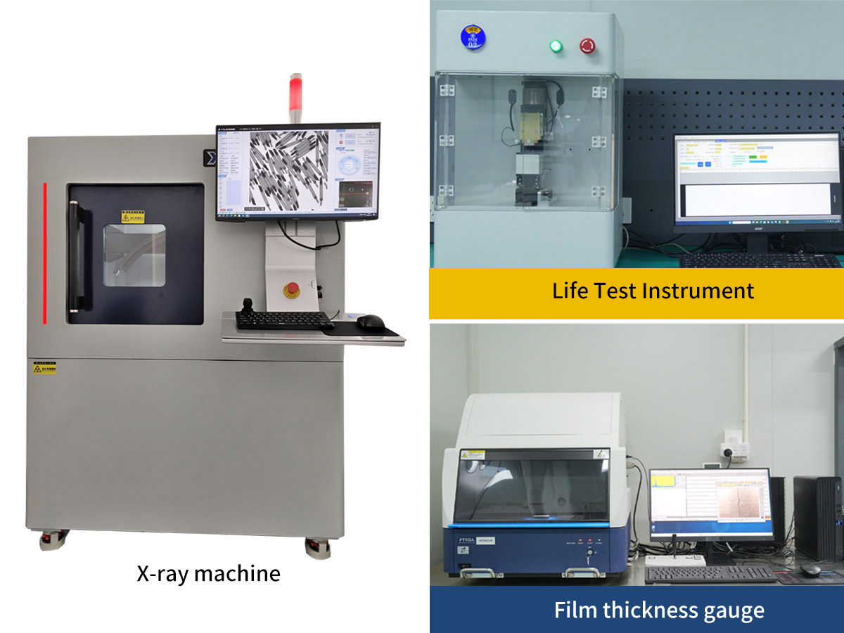
We have a complete set of testing instruments such as industry standard X-ray film thickness measurement equipment and life testing equipment, and perform multiple rigorous quality inspections:
● 100% appearance inspection to avoid mechanical defects;
● Dimensional inspection (accuracy within ± 0.005mm);
● Resistance and elasticity test (generally less than 50mO);
● Life testing (with a lifespan of up to 100000 to 1 million cycles);
● Special test for conducting current;
● Layer by layer inspection and control to ensure stable product accuracy, conductivity, and service life;